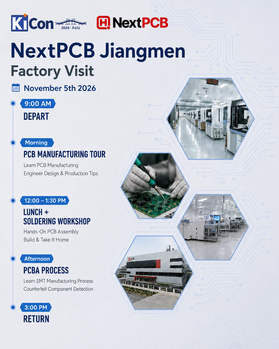
On 5 November, KiCon Asia 2026 takes attendees beyond the design screen and into NextPCB’s modern electronics manufacturing facility in Jiangmen, for a practical look at PCB fabrication, assembly, process control, and the engineering considerations that help designs move smoothly into production.
Schedule
| Time | Activity |
|---|---|
| 9:00 AM | Departure |
| Morning | PCB Manufacturing Tour — Learn about PCB manufacturing, engineering design considerations, and practical production tips |
| 12:00–1:30 PM | Lunch + Soldering Workshop — Take part in hands-on PCB assembly, build a board, and take it home |
| Afternoon | PCBA Process — Explore the SMT manufacturing process and learn about counterfeit component detection |
| 3:00 PM | Return |
Click the image below to view it full-size: